4インチ半絶縁型基板
技術成果
ゼロマイクロチューブ密度制御技術
単結晶形態制御技術
ラップ制御技術
抵抗率制御技術
不純物制御技術
基板ステップ幅制御技術
製品概要
半絶縁炭化ケイ素基板は、半絶縁炭化ケイ素の結晶を切削、研削、研磨、洗浄などの工程を経て加工した単結晶シートです。単結晶基板シートは、第三世代半導体の重要な原料として、ヘテロエピタキシャル成長、デバイス製造などのプロセスを経て、炭化ケイ素ベースのRFデバイスを製造することができ、第3世代半導体産業の発展のための重要な基礎材料です。4インチ製品に対する顧客の要望に応えるため、同社は中国国内・海外の顧客に対し、コスパの高い4インチ半絶縁型基板製品をパッチで提供しています。
川下の製品と応用
半絶縁型炭化ケイ素基板上に窒化ガリウムヘテロジニアスエピタキシャル層を成長させることにより、炭化ケイ素ベースの窒化ガリウムエピタキシャルウェハーが製造され、ウェハー製造、パッケージングテストを通じてマイクロ波RFデバイスに加工することができます。主に5G通信、フェーズドアレイレーダー、ラジオゾンデなどの無線周波数分野で応用されます。


製品仕様書
| Diameter | 99.5 mm - 100.0 mm | |
| Poly-type | 4H | |
| Thickness | 500 μm ± 15 μm | |
| Wafer Orientation | On axis : <0001> ± 0.5° | |
| Micropipe | ≤ 1 cm-2 | |
| Resistivity | ≥1E10 Ω.com | |
| Primary Flat Orientation | {10-10} ± 5.0° | |
| Primary Flat Length | 32.5 mm ± 2.0 mm | |
| Secondary Flat Length | 18.0 mm ± 2.0 mm | |
| Secondary Flat Orientation | Silicon face up: 90° CW. from Prime flat ± 5.0° | |
| Edge Exclusion | 3 mm | |
| LTV / TTV / Bow / Warp | ≤ 2.5 μm/ ≤ 5 μm/ ≤ 15 μm/ ≤ 30 μm | |
| Roughness | Polish Ra ≤ 1 nm | |
| CMP Ra ≤ 0.2 nm | ||
| Edge Cracks By High Intensity Light | - | |
| Hex Plates By High Intensity Light | Cumulative area ≤ 0.05% | |
| Polytype Areas By High Intensity Light | - | |
| Visual Carbon Inclusions | Cumulative area ≤ 0.05% | |
| Silicon Surface Scratches By High Intensity Light | - | |
| Edge Chips High By Intensity Light | None permitted ≥ 0.2 mm width and depth | |
| Silicon Surface Contamination By High Intensity | - | |
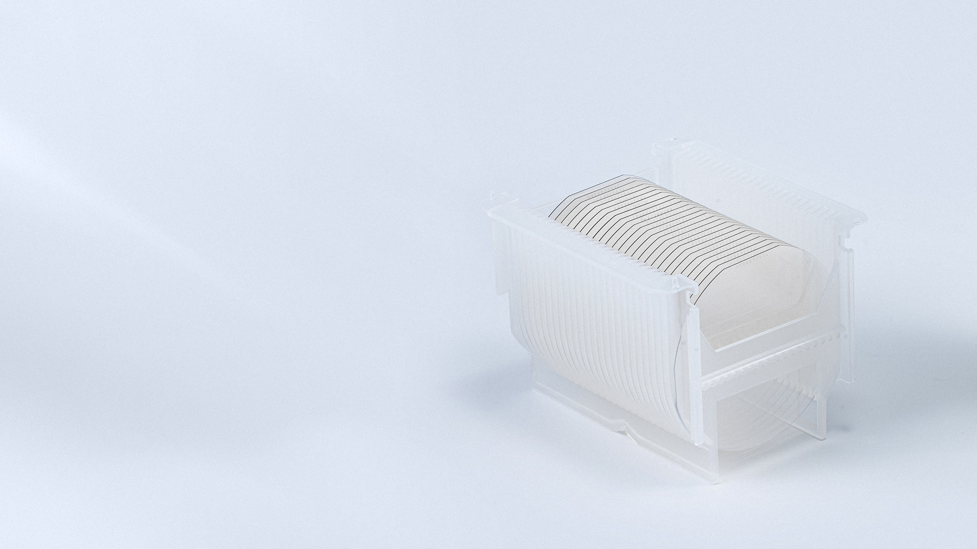
| Packaging | Multi-wafer Cassette Or Single Wafer Container | |
| Diameter | 99.5 mm - 100.0 mm | |
| Poly-type | 4H | |
| Thickness | 500 μm ± 25 μm | |
| Wafer Orientation | On axis : <0001> ± 0.5° | |
| Micropipe | ≤ 15 cm-2 | |
| Resistivity | ≥1E5 Ω.com | |
| Primary Flat Orientation | {10-10} ± 5.0° | |
| Primary Flat Length | 32.5 mm ± 2.0 mm | |
| Secondary Flat Length | 18.0 mm ± 2.0 mm | |
| Secondary Flat Orientation | Silicon face up: 90° CW. from Prime flat ± 5.0° | |
| Edge Exclusion | 3 mm | |
| LTV / TTV / Bow / Warp | ≤ 10 μm/ ≤ 15 μm/ ≤ 25 μm/ ≤ 40 μm | |
| Roughness | Polish Ra ≤ 1 nm | |
| CMP Ra ≤ 0.2 nm | ||
| Edge Cracks By High Intensity Light |
Cumulative length ≤ 10 mm Single length ≤ 2 mm |
|
| Hex Plates By High Intensity Light | Cumulative area ≤ 0.01% | |
| Polytype Areas By High Intensity Light | Cumulative area ≤ 3% | |
| Visual Carbon Inclusions | Cumulative area ≤ 3% | |
| Silicon Surface Scratches By High Intensity Light | Cumulative length ≤1 × wafer diameter | |
| Edge Chips High By Intensity Light | 5 allowed, ≤ 1 mm each | |
| Silicon Surface Contamination By High Intensity | - | |
| Packaging | Multi-wafer Cassette Or Single Wafer Container | |
関連ダウンロード
-
4 Inch Semi-Insulating SiC Substrate Specification.pdf今すぐダウンロード